

 Product
 Brand
Brand Articles
 Tools
Tools
W25Q80DVSNIG: Features, Applications and Datasheet

3/3.3V V SpiFlash® Memory IC SpiFlash® Series 4.9mm mm
Unit Price: $0.164718
Ext Price: $0.16


3/3.3V V SpiFlash® Memory IC SpiFlash® Series 4.9mm mm
Winbond produces an 8-pin serial flash memory device called the W25Q80DVSNIG. This article will introduce its features, applications and datasheet.
W25Q80DVSNIG Description
Systems with limited space, pins, and power can benefit from the storage option offered by the W25Q80DV (8M-bit) Serial Flash memory. Performance and flexibility offered by the 25Q series surpass those of standard SeriaFlash devices. They are perfect for storing voice, text, and data as well as for code shadowing to RAM and direct code execution from Dual/Quad SPlXIP. With a single 2.7V to 3.6V power source, the device can run for as little as 1yA during power down. Every device is available in bundles that save space.There are 4,096 programmable pages with 256 bytes apiece in the W25Q80DV array. One can program up to 256 bytes at a time. Groups of 16 (4KB sector erase), groups of 256 (64KB block erase), groups of 12832KB block erase, or the full chip can be erased (chip erase). There are 16 erasable blocks and 256 erasable sectors on the W25Q80DV, respectively. More flexibility is possible in programs that need to store data and parameters because to the compact 4KB sectors.
The W25Q80DV offers Dua/Quad V0 SPl: Serial Clock, Chip Select, Serial Data 1/00 (DI), 1/02 (WP), and 1/03 (/HOLD), in addition to the usual Serial Peripheral Interface (SPl) and a high performance Dua/Quad output. When employing the Fast Read Dual/Quad 1/0 instructions, comparable clock rates of 208MHz (104MHz x 2) for Dual l/0 and 416MHz (104MHz x 4) for Quad 1/0 are possible due to the support of SPI clock frequencies up to 104MHz. Compared to conventional Asynchronous 8 and 16-bit Parallel Flash memory, these transter speeds can perform better. Additional control flexibility is offered by a Hold pin, Write Protect pin, and programmed write protection with top, bottom, or complement array control.Furthermore, a 64-bit Unique Serial Number is supported by the device for JEDEC standard manufacturer and device identification.
W25Q80DVSNIG Features
Maximum supply voltage of 3.6 V
Maximum active read current of 25 mA
Type of interface: SPI
Clock frequency maximum: 104 MHz
Type of cell: NOR
Sectored Architecture
Boot block: Certainly
Block structure: symmetrical
Specifications
- TypeParameter
- Factory Lead Time10 Weeks
- Mounting Type
The "Mounting Type" in electronic components refers to the method used to attach or connect a component to a circuit board or other substrate, such as through-hole, surface-mount, or panel mount.
Surface Mount - Package / Case
refers to the protective housing that encases an electronic component, providing mechanical support, electrical connections, and thermal management.
8-SOIC (0.154, 3.90mm Width) - Surface Mount
having leads that are designed to be soldered on the side of a circuit board that the body of the component is mounted on.
YES - Memory TypesNon-Volatile
- Operating Temperature
The operating temperature is the range of ambient temperature within which a power supply, or any other electrical equipment, operate in. This ranges from a minimum operating temperature, to a peak or maximum operating temperature, outside which, the power supply may fail.
-40°C~85°C TA - Packaging
Semiconductor package is a carrier / shell used to contain and cover one or more semiconductor components or integrated circuits. The material of the shell can be metal, plastic, glass or ceramic.
Tube - Series
In electronic components, the "Series" refers to a group of products that share similar characteristics, designs, or functionalities, often produced by the same manufacturer. These components within a series typically have common specifications but may vary in terms of voltage, power, or packaging to meet different application needs. The series name helps identify and differentiate between various product lines within a manufacturer's catalog.
SpiFlash® - Published2010
- JESD-609 Code
The "JESD-609 Code" in electronic components refers to a standardized marking code that indicates the lead-free solder composition and finish of electronic components for compliance with environmental regulations.
e3 - Part Status
Parts can have many statuses as they progress through the configuration, analysis, review, and approval stages.
Active - Moisture Sensitivity Level (MSL)
Moisture Sensitivity Level (MSL) is a standardized rating that indicates the susceptibility of electronic components, particularly semiconductors, to moisture-induced damage during storage and the soldering process, defining the allowable exposure time to ambient conditions before they require special handling or baking to prevent failures
3 (168 Hours) - Number of Terminations8
- Terminal Finish
Terminal Finish refers to the surface treatment applied to the terminals or leads of electronic components to enhance their performance and longevity. It can improve solderability, corrosion resistance, and overall reliability of the connection in electronic assemblies. Common finishes include nickel, gold, and tin, each possessing distinct properties suitable for various applications. The choice of terminal finish can significantly impact the durability and effectiveness of electronic devices.
Tin (Sn) - Voltage - Supply
Voltage - Supply refers to the range of voltage levels that an electronic component or circuit is designed to operate with. It indicates the minimum and maximum supply voltage that can be applied for the device to function properly. Providing supply voltages outside this range can lead to malfunction, damage, or reduced performance. This parameter is critical for ensuring compatibility between different components in a circuit.
3V - Terminal Position
In electronic components, the term "Terminal Position" refers to the physical location of the connection points on the component where external electrical connections can be made. These connection points, known as terminals, are typically used to attach wires, leads, or other components to the main body of the electronic component. The terminal position is important for ensuring proper connectivity and functionality of the component within a circuit. It is often specified in technical datasheets or component specifications to help designers and engineers understand how to properly integrate the component into their circuit designs.
DUAL - Peak Reflow Temperature (Cel)
Peak Reflow Temperature (Cel) is a parameter that specifies the maximum temperature at which an electronic component can be exposed during the reflow soldering process. Reflow soldering is a common method used to attach electronic components to a circuit board. The Peak Reflow Temperature is crucial because it ensures that the component is not damaged or degraded during the soldering process. Exceeding the specified Peak Reflow Temperature can lead to issues such as component failure, reduced performance, or even permanent damage to the component. It is important for manufacturers and assemblers to adhere to the recommended Peak Reflow Temperature to ensure the reliability and functionality of the electronic components.
NOT SPECIFIED - Number of Functions1
- Terminal Pitch
The center distance from one pole to the next.
1.27mm - Time@Peak Reflow Temperature-Max (s)
Time@Peak Reflow Temperature-Max (s) refers to the maximum duration that an electronic component can be exposed to the peak reflow temperature during the soldering process, which is crucial for ensuring reliable solder joint formation without damaging the component.
NOT SPECIFIED - JESD-30 Code
JESD-30 Code refers to a standardized descriptive designation system established by JEDEC for semiconductor-device packages. This system provides a systematic method for generating designators that convey essential information about the package's physical characteristics, such as size and shape, which aids in component identification and selection. By using JESD-30 codes, manufacturers and engineers can ensure consistency and clarity in the specification of semiconductor packages across various applications and industries.
R-PDSO-G8 - Qualification Status
An indicator of formal certification of qualifications.
Not Qualified - Power Supplies
an electronic circuit that converts the voltage of an alternating current (AC) into a direct current (DC) voltage.?
3/3.3V - Memory Size
The memory capacity is the amount of data a device can store at any given time in its memory.
8Mb 1M x 8 - Operating Mode
A phase of operation during the operation and maintenance stages of the life cycle of a facility.
SYNCHRONOUS - Clock Frequency
Clock frequency, also known as clock speed, refers to the rate at which a processor or electronic component can execute instructions. It is measured in hertz (Hz) and represents the number of cycles per second that the component can perform. A higher clock frequency typically indicates a faster processing speed and better performance. However, it is important to note that other factors such as architecture, efficiency, and workload also play a significant role in determining the overall performance of a component. In summary, clock frequency is a crucial parameter that influences the speed and efficiency of electronic components in processing data and executing tasks.
104MHz - Memory Format
Memory Format in electronic components refers to the specific organization and structure of data storage within a memory device. It defines how data is stored, accessed, and managed within the memory module. Different memory formats include RAM (Random Access Memory), ROM (Read-Only Memory), and various types of flash memory. The memory format determines the speed, capacity, and functionality of the memory device, and it is crucial for compatibility with other components in a system. Understanding the memory format is essential for selecting the right memory module for a particular application or device.
FLASH - Memory Interface
An external memory interface is a bus protocol for communication from an integrated circuit, such as a microprocessor, to an external memory device located on a circuit board.
SPI - Organization
In the context of electronic components, the parameter "Organization" typically refers to the arrangement or structure of the internal components within a device or system. It can describe how various elements such as transistors, resistors, capacitors, and other components are physically arranged and interconnected on a circuit board or within a semiconductor chip.The organization of electronic components plays a crucial role in determining the functionality, performance, and efficiency of a device. It can impact factors such as signal propagation, power consumption, thermal management, and overall system complexity. Engineers carefully design the organization of components to optimize the operation of electronic devices and ensure reliable performance.Different types of electronic components may have specific organizational requirements based on the intended application and design considerations. For example, integrated circuits may have a highly compact and intricate organization to maximize functionality within a small footprint, while larger electronic systems may have a more modular and distributed organization to facilitate maintenance and scalability.
8MX1 - Memory Width
Memory width refers to the number of bits that can be read or written to memory at one time. It is an important specification in electronic components, particularly in memory devices like RAM and cache. A wider memory width allows for greater data throughput, enabling faster performance as more data can be processed simultaneously. Memory width can vary among different types of memory and can impact both the complexity and efficiency of data handling within electronic systems.
1 - Write Cycle Time - Word, Page
Write Cycle Time - Word, Page refers to the duration required to write data to a specific memory cell or a page of memory in electronic components, particularly in non-volatile memories like Flash or EEPROM. It indicates the time taken to complete a writing operation for a single word or an entire page of data. This parameter is crucial for determining the performance and speed of memory devices in applications where quick data storage is essential. It impacts the overall efficiency in data handling, affecting both read and write speeds in memory-related operations.
3ms - Standby Current-Max
Standby Current-Max refers to the maximum amount of current that an electronic component or device consumes while in a low-power standby mode. This parameter is critical for power management, especially in battery-operated devices, as it indicates how efficiently the device can conserve energy when not actively in use. A lower Standby Current-Max value is typically desirable, as it contributes to longer battery life and reduced energy consumption. Manufacturers specify this value to help engineers select components that meet specific power efficiency requirements in their designs.
0.000005A - Memory Density
Memory density in electronic components refers to the amount of data that can be stored in a given physical space or memory module. It is typically measured in bits or bytes per unit area, such as bits per square inch. Higher memory density means that more data can be stored in a smaller space, which is important for devices with limited physical size or power constraints. Memory density is a key factor in determining the capacity and performance of memory devices, such as RAM, ROM, and flash memory, and is a critical consideration in the design and manufacturing of electronic products.
8388608 bit - Parallel/Serial
The parameter "Parallel/Serial" in electronic components refers to the method of data transmission or communication within the component. In parallel communication, multiple bits of data are transmitted simultaneously over multiple channels or wires. This allows for faster data transfer rates but requires more physical connections and can be more susceptible to signal interference.On the other hand, in serial communication, data is transmitted sequentially over a single channel or wire. While serial communication may have slower data transfer rates compared to parallel communication, it is more cost-effective, requires fewer connections, and is less prone to signal interference.The choice between parallel and serial communication depends on the specific requirements of the electronic component and the overall system design, balancing factors such as speed, cost, complexity, and reliability.
SERIAL - Programming Voltage
A special high-voltage supply that supplies the potential and energy for altering the state of certain nonvolatile memory arrays. On some devices, the presence of VPP also acts as a program enable signal (P).
3V - Serial Bus Type
Serial bus type refers to the method by which data is transmitted between components in an electronic system using a serial communication protocol. It involves the sequential transfer of data bits over a single channel or wire, allowing for a reduced number of interconnections compared to parallel communication. Common examples of serial bus types include I2C, SPI, USB, and UART, each with its own specific protocol and applications. The choice of serial bus type can affect the speed, complexity, and power consumption of the communication between devices.
SPI - Endurance
In electronic components, "Endurance" refers to the ability of a component to withstand repeated cycles of operation without degradation in performance or failure. It is a crucial parameter, especially in components that are subjected to frequent switching or high levels of stress during operation. Endurance testing is often conducted to evaluate the reliability and durability of electronic components under real-world conditions. Components with high endurance ratings are more likely to have a longer lifespan and provide consistent performance over time. Manufacturers typically provide endurance specifications in datasheets to help engineers and designers select components that meet the required durability for their applications.
100000 Write/Erase Cycles - Data Retention Time-Min
The parameter "Data Retention Time-Min" in electronic components refers to the minimum amount of time that data can be stored in a non-volatile memory device without requiring a refresh or rewrite operation to maintain its integrity. This parameter is crucial for applications where data integrity and reliability are essential, such as in embedded systems, IoT devices, and critical infrastructure. A longer data retention time indicates a more stable memory device that can retain data for extended periods without degradation or loss. It is important to consider the data retention time when selecting memory components for specific applications to ensure data reliability and longevity.
20 - Write Protection
Write protection is a feature found in electronic components, such as memory devices, that prevents data from being modified or erased. When write protection is enabled, the data stored in the component is locked and cannot be altered, ensuring the integrity and security of the information. This feature is commonly used in devices like USB flash drives, SD cards, and EEPROMs to prevent accidental data loss or unauthorized access. Write protection can be implemented through hardware mechanisms, such as physical switches or jumpers, or through software settings that restrict write access to the component.
HARDWARE/SOFTWARE - Voltage - Supply (Max)
Voltage - Supply (Max) is a parameter in electronic components that specifies the maximum voltage that can be safely applied to the component for proper operation. This parameter is crucial for ensuring the component's longevity and preventing damage due to overvoltage conditions. Exceeding the maximum supply voltage can lead to component failure, reduced performance, or even permanent damage. Designers must carefully consider this parameter when selecting components and designing circuits to ensure reliable and safe operation within the specified voltage limits.
3.6V - Voltage - Supply (Min)
Voltage - Supply (Min) is a parameter in electronic components that specifies the minimum voltage required for the component to operate within its specified performance range. This parameter indicates the lowest voltage level that can be safely applied to the component without causing malfunctions or damage. It is crucial to ensure that the supply voltage provided to the component is equal to or higher than the specified minimum voltage to guarantee proper functionality and reliability. Failure to meet this requirement may result in erratic behavior, reduced performance, or even permanent damage to the component.
2.7V - Ambient Temperature Range High
This varies from person to person, but it is somewhere between 68 and 77 degrees F on average. The temperature setting that is comfortable for an individual may fluctuate with humidity and outside temperature as well. The temperature of an air conditioned room can also be considered ambient temperature.
85°C - Height1.75mm
- Length4.9mm
- Width3.9mm
- RoHS Status
RoHS means “Restriction of Certain Hazardous Substances” in the “Hazardous Substances Directive” in electrical and electronic equipment.
ROHS3 Compliant
W25Q80DVSNIG Pinout
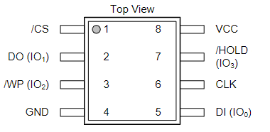
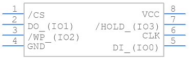
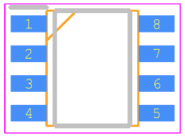
W25Q80DVSNIG CAD Model
Symbol
Footprint
3D Model

W25Q80DVSNIG Alternatives
Part Number | Description | Manufacturer |
W25Q80DVSNIGT | Flash, 1MX8, PDSO8, SOIC-8 | Winbond Electronics Corp |
W25Q80DVSNIG Applications
Applications that require data and parameter storage
W25Q80DVSNIG Manufacturer
Winbond Electronics Corporation is a Taiwan-based corporation that was founded in 19871. It is a leading global supplier of semiconductor memory solutions. The company produces semiconductors and several types of integrated circuits (ICs) including dynamic random-access memory, static random-access memory, serial flash, microcontrollers, and Super I/O chips. Winbond is the largest brand-name IC supplier in Taiwan and one of the biggest suppliers of semiconductor solutions worldwide.
The main business groups of Winbond include: DRAM Product, NOR Flash and Memory IC Manufacturing. The company provides customer-driven memory solutions backed by the expert capabilities of product design, R&D, manufacturing, and sales services. Winbond’s headquarters are in Central Taiwan Science Park, Taiwan and it has subsidies in America, Japan, and Hong Kong.
Parts with Similar Specs
- ImagePart NumberManufacturerPackage / CasePower SuppliesTerminal PitchOperating ModeSupply Voltage-Min (Vsup)Terminal PositionJESD-30 CodeNumber of TerminationsView Compare
![W25Q80DVSNIG]()
W25Q80DVSNIG
8-SOIC (0.154, 3.90mm Width)
3/3.3 V
1.27 mm
SYNCHRONOUS
2.7 V
DUAL
R-PDSO-G8
8
![MX25L1606EM1I-12G]()
8-SOIC (0.154, 3.90mm Width)
3/3.3 V
1.27 mm
SYNCHRONOUS
2.7 V
DUAL
R-PDSO-G8
8
![MX25L512EMI-10G]()
8-SOIC (0.209, 5.30mm Width)
3/3.3 V
1.27 mm
SYNCHRONOUS
2.7 V
DUAL
R-PDSO-G8
8
![MX25L8006EM1I-12G]()
8-SOIC (0.154, 3.90mm Width)
3/3.3 V
1.27 mm
SYNCHRONOUS
2.7 V
DUAL
R-PDSO-G8
8
![MX25L8006EM2I-12G]()
SOIC
3/3.3 V
1.27 mm
SYNCHRONOUS
2.7 V
DUAL
R-PDSO-G8
8


Datasheet PDF
- Datasheets :
- PCN Packaging :
What is Winbond Electronics W25Q80DVSNIG?
Winbond Electronics' W25Q80DVSNIG is a 8Mbit SPI-Quad I/O 104 MHz 8-SOIC NOR Memory IC. It has a 24-bit address bus width and a sector size of 4Kbyte x 256.
 LIS2DE12TR Motion Sensor: Three-Axis Accelerometer, Datasheet, Application Hint
26 February 20222373
 SigmaDSP Audio Processors 294.912 MHz Performance: Datasheet, Pinout, and Design Analysis
12 February 20261261
 MC1458 Dual Op-Amp: Specifications, Design Limitations, and Modern Replacement Options
08 June 2026655
 ADM3222ANZ Transceivers: Pinout, Specification, Datasheet
27 May 2021640
 TPS7B6950QDBVRQ1 Regulator: Equivalents, Pinout
25 March 2022909
 TDA7266 Amplifier: Datasheet, Circuit, Equivalents
27 September 202139530
 Stop Struggling with Weak Sensor Signals: AD8338 Makes High-Gain Amplification Dead Simple
19 March 2026281
 TDA2030 Audio Amplifier: Datasheet, Pinout and Equivalents
15 September 202160814
 Basics of Phase Change Memory
05 February 20219123
 Basic Introduction to Power Amplifier
09 January 202610980
 Top 5 Microcontrollers Defining IoT, Edge AI, and Power Efficiency in 2026: Sourcing and Selection Guide
15 August 2026800
 Power Management ICs Trends 2026: AI Demand, Supply Risks, and Sourcing Strategies
06 July 20261513
 Basis of Fiber Optic and Fiber Optic Communication
22 October 20215480
 Semiconductor Devices: Impact on IoT and Modern Communication (Part-1)
22 July 20242774
 What is RF Power Amplifier?
08 November 202512847
 Role of Solar Energy in Wide-Band Gap Devices for Photovoltaic Applications
15 March 20244766
Winbond Electronics
In Stock: 20488
Minimum: 1 Multiples: 1
Qty
Unit Price
Ext Price
1
$0.164718
$0.16
10
$0.155394
$1.55
100
$0.146598
$14.66
500
$0.138300
$69.15
1000
$0.130472
$130.47
Not the price you want? Send RFQ Now and we'll contact you ASAP.
Inquire for More Quantity
![W25Q128JVSIQ]() W25Q128JVSIQ
W25Q128JVSIQWinbond Electronics
![W25Q80DVSSIG]() W25Q80DVSSIG
W25Q80DVSSIGWinbond Electronics
![W9825G6KH-6]() W9825G6KH-6
W9825G6KH-6Winbond Electronics
![W27C512-45Z]() W27C512-45Z
W27C512-45ZWinbond Electronics
![W25Q32JWBYIQ TR]() W25Q32JWBYIQ TR
W25Q32JWBYIQ TRWinbond Electronics
![W9812G6KH-6]() W9812G6KH-6
W9812G6KH-6Winbond Electronics
![W25Q64FVSSIG]() W25Q64FVSSIG
W25Q64FVSSIGWinbond Electronics
![W25Q64JVSSIQ]() W25Q64JVSSIQ
W25Q64JVSSIQWinbond Electronics
![W25X40CLSNIG]() W25X40CLSNIG
W25X40CLSNIGWinbond Electronics
![W25Q128FVSIG]() W25Q128FVSIG
W25Q128FVSIGWinbond Electronics


