
 Product
 Brand
Brand Articles
 Tools
Tools
IXBK55N300 Monolithic Bipolar MOS Transistor: Package, Pinout, and Datasheet


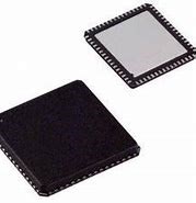
Trans IGBT Chip N-CH 3KV 130A 3-Pin(3 Tab) TO-264
IXBK55N300 is a Monolithic Bipolar MOS Transistor. This article mainly introduces package, pinout, datasheet and other detailed information about IXYS IXBK55N300.

MOSFET BJT or IGBT - Brief comparison Basic components #004
IXBK55N300 Description
IXBK55N300 is a High Voltage, High Gain BiMOSFETTM, Monolithic Bipolar MOS Transistor.
• VCES = 3000V
• IC110 = 55A
• VCE(sat) ≤ 3.2V
IXBK55N300 Pinout
The following figure is IXBK55N300 Pinout.

Pinout
IXBK55N300 CAD Model
The followings show IXBK55N300 Symbol, Footprint and 3D Model.

Symbol

Footprint

3D Model
IXBK55N300 Features
• High Blocking Voltage
• International Standard Packages
• Low Conduction Losses
• High Current Handling Capability
• MOS Gate Turn-On
- Drive Simplicity
• Easy to Mount
• Space Savings
• High Power Density
Specifications
- TypeParameter
- Factory Lead Time28 Weeks
- Mount
In electronic components, the term "Mount" typically refers to the method or process of physically attaching or fixing a component onto a circuit board or other electronic device. This can involve soldering, adhesive bonding, or other techniques to secure the component in place. The mounting process is crucial for ensuring proper electrical connections and mechanical stability within the electronic system. Different components may have specific mounting requirements based on their size, shape, and function, and manufacturers provide guidelines for proper mounting procedures to ensure optimal performance and reliability of the electronic device.
Through Hole - Mounting Type
The "Mounting Type" in electronic components refers to the method used to attach or connect a component to a circuit board or other substrate, such as through-hole, surface-mount, or panel mount.
Through Hole - Package / Case
refers to the protective housing that encases an electronic component, providing mechanical support, electrical connections, and thermal management.
TO-264-3, TO-264AA - Transistor Element Material
The "Transistor Element Material" parameter in electronic components refers to the material used to construct the transistor within the component. Transistors are semiconductor devices that amplify or switch electronic signals and are a fundamental building block in electronic circuits. The material used for the transistor element can significantly impact the performance and characteristics of the component. Common materials used for transistor elements include silicon, germanium, and gallium arsenide, each with its own unique properties and suitability for different applications. The choice of transistor element material is crucial in designing electronic components to meet specific performance requirements such as speed, power efficiency, and temperature tolerance.
SILICON - Collector-Emitter Breakdown Voltage3kV
- Number of Elements1
- Operating Temperature
The operating temperature is the range of ambient temperature within which a power supply, or any other electrical equipment, operate in. This ranges from a minimum operating temperature, to a peak or maximum operating temperature, outside which, the power supply may fail.
-55°C~150°C TJ - Packaging
Semiconductor package is a carrier / shell used to contain and cover one or more semiconductor components or integrated circuits. The material of the shell can be metal, plastic, glass or ceramic.
Tube - Series
In electronic components, the "Series" refers to a group of products that share similar characteristics, designs, or functionalities, often produced by the same manufacturer. These components within a series typically have common specifications but may vary in terms of voltage, power, or packaging to meet different application needs. The series name helps identify and differentiate between various product lines within a manufacturer's catalog.
BIMOSFET™ - Published2009
- JESD-609 Code
The "JESD-609 Code" in electronic components refers to a standardized marking code that indicates the lead-free solder composition and finish of electronic components for compliance with environmental regulations.
e1 - Pbfree Code
The "Pbfree Code" parameter in electronic components refers to the code or marking used to indicate that the component is lead-free. Lead (Pb) is a toxic substance that has been widely used in electronic components for many years, but due to environmental concerns, there has been a shift towards lead-free alternatives. The Pbfree Code helps manufacturers and users easily identify components that do not contain lead, ensuring compliance with regulations and promoting environmentally friendly practices. It is important to pay attention to the Pbfree Code when selecting electronic components to ensure they meet the necessary requirements for lead-free applications.
yes - Part Status
Parts can have many statuses as they progress through the configuration, analysis, review, and approval stages.
Active - Moisture Sensitivity Level (MSL)
Moisture Sensitivity Level (MSL) is a standardized rating that indicates the susceptibility of electronic components, particularly semiconductors, to moisture-induced damage during storage and the soldering process, defining the allowable exposure time to ambient conditions before they require special handling or baking to prevent failures
1 (Unlimited) - Number of Terminations3
- Terminal Finish
Terminal Finish refers to the surface treatment applied to the terminals or leads of electronic components to enhance their performance and longevity. It can improve solderability, corrosion resistance, and overall reliability of the connection in electronic assemblies. Common finishes include nickel, gold, and tin, each possessing distinct properties suitable for various applications. The choice of terminal finish can significantly impact the durability and effectiveness of electronic devices.
Tin/Silver/Copper (Sn/Ag/Cu) - Additional Feature
Any Feature, including a modified Existing Feature, that is not an Existing Feature.
LOW CONDUCTION LOSS - Max Power Dissipation
The maximum power that the MOSFET can dissipate continuously under the specified thermal conditions.
625W - Pin Count
a count of all of the component leads (or pins)
3 - JESD-30 Code
JESD-30 Code refers to a standardized descriptive designation system established by JEDEC for semiconductor-device packages. This system provides a systematic method for generating designators that convey essential information about the package's physical characteristics, such as size and shape, which aids in component identification and selection. By using JESD-30 codes, manufacturers and engineers can ensure consistency and clarity in the specification of semiconductor packages across various applications and industries.
R-PSFM-T3 - Element Configuration
The distribution of electrons of an atom or molecule (or other physical structure) in atomic or molecular orbitals.
Single - Case Connection
Case Connection refers to the method by which an electronic component's case or housing is connected to the electrical circuit. This connection is important for grounding purposes, mechanical stability, and heat dissipation. The case connection can vary depending on the type of component and its intended application. It is crucial to ensure a secure and reliable case connection to maintain the overall performance and safety of the electronic device.
COLLECTOR - Input Type
Input type in electronic components refers to the classification of the signal or data that a component can accept for processing or conversion. It indicates whether the input is analog, digital, or a specific format such as TTL or CMOS. Understanding input type is crucial for ensuring compatibility between different electronic devices and circuits, as it determines how signals are interpreted and interacted with.
Standard - Power - Max
Power - Max is a parameter that specifies the maximum amount of power that an electronic component can handle without being damaged. It is typically measured in watts and indicates the upper limit of power that can be safely supplied to the component. Exceeding the maximum power rating can lead to overheating, malfunction, or permanent damage to the component. It is important to consider the power-max rating when designing circuits or systems to ensure proper operation and longevity of the electronic components.
625W - Transistor Application
In the context of electronic components, the parameter "Transistor Application" refers to the specific purpose or function for which a transistor is designed and used. Transistors are semiconductor devices that can amplify or switch electronic signals and are commonly used in various electronic circuits. The application of a transistor can vary widely depending on its design and characteristics, such as whether it is intended for audio amplification, digital logic, power control, or radio frequency applications. Understanding the transistor application is important for selecting the right type of transistor for a particular circuit or system to ensure optimal performance and functionality.
POWER CONTROL - Polarity/Channel Type
In electronic components, the parameter "Polarity/Channel Type" refers to the characteristic that determines the direction of current flow or the type of signal that can be accommodated by the component. For components like diodes and transistors, polarity indicates the direction in which current can flow through the component, such as forward bias or reverse bias for diodes. For components like MOSFETs or JFETs, the channel type refers to whether the component is an N-channel or P-channel device, which determines the type of charge carriers that carry current through the component. Understanding the polarity or channel type of a component is crucial for proper circuit design and ensuring that the component is connected correctly to achieve the desired functionality.
N-CHANNEL - Collector Emitter Voltage (VCEO)
Collector-Emitter Voltage (VCEO) is a key parameter in electronic components, particularly in transistors. It refers to the maximum voltage that can be applied between the collector and emitter terminals of a transistor while the base terminal is open or not conducting. Exceeding this voltage limit can lead to breakdown and potential damage to the transistor. VCEO is crucial for ensuring the safe and reliable operation of the transistor within its specified limits. Designers must carefully consider VCEO when selecting transistors for a circuit to prevent overvoltage conditions that could compromise the performance and longevity of the component.
3.2V - Max Collector Current
Max Collector Current is a parameter used to specify the maximum amount of current that can safely flow through the collector terminal of a transistor or other electronic component without causing damage. It is typically expressed in units of amperes (A) and is an important consideration when designing circuits to ensure that the component operates within its safe operating limits. Exceeding the specified max collector current can lead to overheating, degradation of performance, or even permanent damage to the component. Designers must carefully consider this parameter when selecting components and designing circuits to ensure reliable and safe operation.
130A - Reverse Recovery Time
Reverse Recovery Time is a key parameter in semiconductor devices, particularly diodes and transistors. It refers to the time taken for a diode or transistor to switch from conducting in the forward direction to blocking in the reverse direction when the polarity of the voltage across the device is reversed. This parameter is crucial in applications where fast switching speeds are required, as a shorter reverse recovery time allows for quicker response times and improved efficiency. Reverse Recovery Time is typically specified in datasheets for electronic components and is an important consideration in circuit design to ensure optimal performance and reliability.
1.9 μs - Voltage - Collector Emitter Breakdown (Max)
Voltage - Collector Emitter Breakdown (Max) is a parameter that specifies the maximum voltage that can be applied between the collector and emitter terminals of a transistor or other semiconductor device before it breaks down and allows excessive current to flow. This parameter is crucial for ensuring the safe and reliable operation of the component within its specified limits. Exceeding the maximum breakdown voltage can lead to permanent damage or failure of the device. Designers and engineers must carefully consider this parameter when selecting components for their circuits to prevent potential issues and ensure proper functionality.
3000V - Turn On Time
The time that it takes a gate circuit to allow a current to reach its full value.
637 ns - Vce(on) (Max) @ Vge, Ic
The parameter "Vce(on) (Max) @ Vge, Ic" in electronic components refers to the maximum voltage drop across the collector-emitter junction of a power transistor when it is in the on-state. This parameter is specified at a certain gate-emitter voltage (Vge) and collector current (Ic). It indicates the maximum voltage that can be sustained across the collector-emitter terminals while the transistor is conducting current. This parameter is important for determining the power dissipation and efficiency of the transistor in a circuit, as well as for ensuring proper operation and reliability of the component.
3.2V @ 15V, 55A - Turn Off Time-Nom (toff)
Turn Off Time-Nom (toff) is a parameter in electronic components, particularly in devices like transistors and diodes. It refers to the time taken for the device to switch from the on state to the off state when a control signal is applied. This parameter is crucial in determining the switching speed and efficiency of the component. A shorter turn-off time generally indicates faster switching speeds, which can be important in applications where rapid response times are required. Manufacturers provide this specification to help engineers and designers select the right components for their specific needs and ensure optimal performance in their circuits.
475 ns - Gate Charge
the amount of charge that needs to be injected into the gate electrode to turn ON (drive) the MOSFET.
335nC - Current - Collector Pulsed (Icm)
The parameter "Current - Collector Pulsed (Icm)" in electronic components refers to the maximum allowable collector current that the component can handle when operating in a pulsed mode. This parameter is crucial for devices such as transistors and power amplifiers that may experience short bursts of high current during operation. Exceeding the specified Icm rating can lead to overheating, device failure, or even permanent damage. Designers must carefully consider this parameter when selecting components to ensure reliable and safe operation within the specified limits.
600A - Gate-Emitter Voltage-Max
The "Gate-Emitter Voltage-Max" parameter is a specification commonly found in field-effect transistors (FETs) and insulated gate bipolar transistors (IGBTs). It refers to the maximum allowable voltage that can be applied between the gate and emitter terminals of the device without causing damage. Exceeding this voltage limit can lead to breakdown of the gate oxide layer or other critical components, resulting in potential device failure.This parameter is crucial for ensuring the reliable operation of the transistor and preventing overvoltage conditions that could compromise its performance or longevity. Designers must carefully consider the Gate-Emitter Voltage-Max specification when selecting and using these components in electronic circuits to avoid exceeding the specified limits and causing damage to the device. It is typically provided in the datasheet of the component and serves as a key parameter for proper device operation within safe operating conditions.
25V - Gate-Emitter Thr Voltage-Max
Gate-Emitter Threshold Voltage-Max refers to the maximum voltage required between the gate and emitter terminals of a transistor to begin conducting. It is a critical parameter in defining the operating characteristics of transistors, particularly in field-effect transistors and bipolar junction transistors. This threshold voltage indicates the point at which the transistor will start to turn on and allows current to flow from the collector to the emitter. Understanding this parameter is essential for ensuring proper biasing and operation in electronic circuits.
5V - Radiation Hardening
Radiation hardening is the process of making electronic components and circuits resistant to damage or malfunction caused by high levels of ionizing radiation, especially for environments in outer space (especially beyond the low Earth orbit), around nuclear reactors and particle accelerators, or during nuclear accidents or nuclear warfare.
No - RoHS Status
RoHS means “Restriction of Certain Hazardous Substances” in the “Hazardous Substances Directive” in electrical and electronic equipment.
ROHS3 Compliant - Lead Free
Lead Free is a term used to describe electronic components that do not contain lead as part of their composition. Lead is a toxic material that can have harmful effects on human health and the environment, so the electronics industry has been moving towards lead-free components to reduce these risks. Lead-free components are typically made using alternative materials such as silver, copper, and tin. Manufacturers must comply with regulations such as the Restriction of Hazardous Substances (RoHS) directive to ensure that their products are lead-free and environmentally friendly.
Lead Free
Parts with Similar Specs
- ImagePart NumberManufacturerMountPackage / CaseCollector Emitter Breakdown VoltageVoltage - Collector Emitter Breakdown (Max)Max Collector CurrentMax Power DissipationReverse Recovery TimeRoHS StatusView Compare
![IXBK55N300]()
IXBK55N300
Through Hole
TO-264-3, TO-264AA
3 kV
3000V
130 A
625 W
1.9 μs
ROHS3 Compliant
![FGL40N120ANDTU]()
Through Hole
TO-264-3, TO-264AA
1.2 kV
1200V
64 A
500 W
112 ns
ROHS3 Compliant
![IXBK75N170]()
Through Hole
TO-264-3, TO-264AA
600 V
-
160 A
250 W
95 ns
ROHS3 Compliant
![SGL160N60UFDTU]()
Through Hole
TO-264-3, TO-264AA
600 V
-
80 A
250 W
100ns
ROHS3 Compliant
![SGL50N60RUFDTU]()
Through Hole
TO-264-3, TO-264AA
1.7 kV
1700V
200 A
1.04 kW
1.5 μs
ROHS3 Compliant


IXBK55N300 Applications
• Uninterruptible Power Supplies (UPS)
• Switch-Mode and Resonant-Mode Power Supplies
• Capacitor Discharge Circuits
• Laser Generators
IXBK55N300 Package
The following figure is IXBK55N300 Package.

TO-264 Outline

PLUS 247TM Outline
IXBK55N300 Manufacturer
Littelfuse's power semiconductor portfolio has grown dramatically as a result of the acquisition of IXYS, with solutions spanning a wide range of technologies. Customers will benefit from the greatest technology and enhanced, differentiated capabilities in target markets and geographies, as well as better industry access and growth prospects, thanks to this comprehensive portfolio. As Littelfuse Inc. integrates them into their portfolio of world-class products, the three business units listed below will gradually combine into IXYS a Littelfuse Technology. IXYS. a Littelfuse Technology company has established itself as a leading power semiconductor maker around the world. Low on-resistance Power MOSFETs , Ultra Fast switching IGBTs, Fast Recovery Diodes (FREDs), SCR and Diode Modules, Rectifier Bridges, and Power Interface ICs are among the company's specialized power semiconductors, integrated circuits, and RF power products for applications in the industrial, transportation, telecommunications, computer, medical, consumer, and cleantech markets. IXYS Integrated Circuits Division, formerly Clare, Inc., is a division of Littelfuse that designs, manufactures, and sells high-voltage integrated circuits (ICs) and optically isolated Solid State Relays (OptoMOS®) for the communication, industrial, power, and consumer industries. They have become a significant supplier to the telecommunications, security, utility metering, and industrial control industries as a pioneer in the creation of Solid State Relays (SSRs).
In many applications, SSR solutions from IXYS Integrated Circuits Division are rapidly replacing older electromechanical devices and improving overall system performance. They're still working on new leadership products with better integration and electrical performance. The DE-Series package continues to be used by IXYS RF/Littelfuse to supply high-performance MOSFETs, drivers, and integrated modules. IXYS /design Littelfuse's team created die particularly for use in their DE-Series package, leveraging industry-standard packaging to make their technology available to a larger range of applications and markets.
Trend Analysis
Datasheet PDF
- Datasheets :
 PIC16F917IML Microcontroller: Technical Specifications and Features Overview
29 February 2024142
 Infineon IRLML2502TRPBF price hacks every buyer should know
18 August 2025246
 SMBJ60CA TVs Diodes: System, Pinout, and Datasheet
14 February 20222550
 TPS7A11 Voltage Regulator: Pinout, Datasheet, Alternatives
06 October 20221008
 TDA7293 DMOS Audio Amplifier: Datasheet, TDA7293 vs. TDA7294
03 December 202115615
 IRF830 Power MOSFET: Pinout, Datasheet, and Test Circuit
14 July 20215098
 AD9520-0BCPZ Clock Generators: Pinout, Feature, Specification
14 August 2024520
 PT4115 High Brightness LED Driver: 30A, 1.2V Step-down Driver, Equivalent and Pinout
06 January 202213979
 How to Properly Install TVS Diodes in Your PCB Design
11 July 20253788
 Semiconductor Memory Market to See More Significant Price Declines
17 August 20222235
 US Set to Close Loopholes in AI Chip Export Restrictions to China
23 October 20231778
 The Comprehensive Guide to MOSFETs: Principles, Types, and Parameters (2026 Edition)
16 January 202617341
 Good news | Warm Congratulations to UTMEL Electronic for Obtaining the Letter of Authorization from XKB Connectivity
21 July 20253299
 What is Digital Signal Processing (DSP)?
17 March 20224365
 Analysis of Resistors in Series and Parallel
16 October 202518047
 What are the Commonly Used Anti-Jamming Technologies for Sensors?
27 December 20211297
IXYS
In Stock: 118
United States
China
Canada
Japan
Russia
Germany
United Kingdom
Singapore
Italy
Hong Kong(China)
Taiwan(China)
France
Korea
Mexico
Netherlands
Malaysia
Austria
Spain
Switzerland
Poland
Thailand
Vietnam
India
United Arab Emirates
Afghanistan
Åland Islands
Albania
Algeria
American Samoa
Andorra
Angola
Anguilla
Antigua & Barbuda
Argentina
Armenia
Aruba
Australia
Azerbaijan
Bahamas
Bahrain
Bangladesh
Barbados
Belarus
Belgium
Belize
Benin
Bermuda
Bhutan
Bolivia
Bonaire, Sint Eustatius and Saba
Bosnia & Herzegovina
Botswana
Brazil
British Indian Ocean Territory
British Virgin Islands
Brunei
Bulgaria
Burkina Faso
Burundi
Cabo Verde
Cambodia
Cameroon
Cayman Islands
Central African Republic
Chad
Chile
Christmas Island
Cocos (Keeling) Islands
Colombia
Comoros
Congo
Congo (DRC)
Cook Islands
Costa Rica
Côte d’Ivoire
Croatia
Cuba
Curaçao
Cyprus
Czechia
Denmark
Djibouti
Dominica
Dominican Republic
Ecuador
Egypt
El Salvador
Equatorial Guinea
Eritrea
Estonia
Eswatini
Ethiopia
Falkland Islands
Faroe Islands
Fiji
Finland
French Guiana
French Polynesia
Gabon
Gambia
Georgia
Ghana
Gibraltar
Greece
Greenland
Grenada
Guadeloupe
Guam
Guatemala
Guernsey
Guinea
Guinea-Bissau
Guyana
Haiti
Honduras
Hungary
Iceland
Indonesia
Iran
Iraq
Ireland
Isle of Man
Israel
Jamaica
Jersey
Jordan
Kazakhstan
Kenya
Kiribati
Kosovo
Kuwait
Kyrgyzstan
Laos
Latvia
Lebanon
Lesotho
Liberia
Libya
Liechtenstein
Lithuania
Luxembourg
Macao(China)
Madagascar
Malawi
Maldives
Mali
Malta
Marshall Islands
Martinique
Mauritania
Mauritius
Mayotte
Micronesia
Moldova
Monaco
Mongolia
Montenegro
Montserrat
Morocco
Mozambique
Myanmar
Namibia
Nauru
Nepal
New Caledonia
New Zealand
Nicaragua
Niger
Nigeria
Niue
Norfolk Island
North Korea
North Macedonia
Northern Mariana Islands
Norway
Oman
Pakistan
Palau
Palestinian Authority
Panama
Papua New Guinea
Paraguay
Peru
Philippines
Pitcairn Islands
Portugal
Puerto Rico
Qatar
Réunion
Romania
Rwanda
Samoa
San Marino
São Tomé & Príncipe
Saudi Arabia
Senegal
Serbia
Seychelles
Sierra Leone
Sint Maarten
Slovakia
Slovenia
Solomon Islands
Somalia
South Africa
South Sudan
Sri Lanka
St Helena, Ascension, Tristan da Cunha
St. Barthélemy
St. Kitts & Nevis
St. Lucia
St. Martin
St. Pierre & Miquelon
St. Vincent & Grenadines
Sudan
Suriname
Svalbard & Jan Mayen
Sweden
Syria
Tajikistan
Tanzania
Timor-Leste
Togo
Tokelau
Tonga
Trinidad & Tobago
Tunisia
Turkey
Turkmenistan
Turks & Caicos Islands
Tuvalu
U.S. Outlying Islands
U.S. Virgin Islands
Uganda
Ukraine
Uruguay
Uzbekistan
Vanuatu
Vatican City
Venezuela
Wallis & Futuna
Yemen
Zambia
Zimbabwe
![IXGH60N60C3D1]() IXGH60N60C3D1
IXGH60N60C3D1IXYS
![IXLF19N250A]() IXLF19N250A
IXLF19N250AIXYS
![IXGH40N120C3D1]() IXGH40N120C3D1
IXGH40N120C3D1IXYS
![IXGH48N60B3D1]() IXGH48N60B3D1
IXGH48N60B3D1IXYS
![IXGH72N60A3]() IXGH72N60A3
IXGH72N60A3IXYS
![IXGP20N120A3]() IXGP20N120A3
IXGP20N120A3IXYS
![IXXH75N60C3D1]() IXXH75N60C3D1
IXXH75N60C3D1IXYS
![IXGH6N170A]() IXGH6N170A
IXGH6N170AIXYS
![IXGH16N170A]() IXGH16N170A
IXGH16N170AIXYS
![IXGA48N60A3]() IXGA48N60A3
IXGA48N60A3IXYS


